[ China Instrument Network Instrument Research and Development ] Recently, Hu Weida, Chen Xiaoshuang and Lu Wei, the State Key Laboratory of Infrared Physics, Shanghai Institute of Technical Physics, Chinese Academy of Sciences, made progress in the study of room temperature nanowire single photon detectors. Researchers at the lab used the Photogating effect of nanowires for the first time to detect single photons at room temperature on a single nanowire. The related results were published in the international journal Nano Letters (DOI: 10.1021/acs.nanolett.8b01795, impact factor 12.08) under the title "Room-Temperature Single-Photon Detector Based on Single Nanowire". The first author of the thesis is Dr. Luo Wenjin.
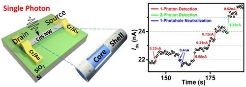
Room temperature nanowire single photon detector structure diagram and single photon response visual map
Single-photon detectors rely on their extremely sensitive detection capabilities to record individual photons—a quantum unit that is widely used in many fields, such as precision analysis, bioluminescence, high-energy physics, astronomical ranging, especially in quantum key distribution. Indispensable in the system. Although single-photon detectors have been developed for many years and have a wide variety, there are still many shortcomings. First, the operating conditions of traditional single-photon detectors are relatively harsh. For example, photomultiplier tubes and avalanche diodes operating in Geiger mode require driving voltages of tens of volts or even thousands of volts, while superconducting single-photon detectors require several Kelvin. Extremely low temperature environment. Second, most single-photon detectors rely on high-quality material growth, require molecular beam epitaxy and other equipment, and the cost of device fabrication is high. In addition, there are still a handful of single-photon detectors with photon number resolution, and this resolvability is critical to many protocols for communication technology. Therefore, there is an urgent need to study photodetectors with room temperature, low cost and simultaneous photon number resolution to meet the needs of single photon detection in many fields of modern science and engineering.
What are the advantages of nanowires for single-photon detection at room temperature?
Semiconductor nanowires are quasi-one-dimensional quantum structures with large surface area/volume ratios and special physical and chemical properties such as light, electricity and magnetism. In recent years, many research work has reported that the performance of nanowire detectors can be improved by manipulating the surface states of nanowires. Among them, the photoinduced effect of the photogating effect has been widely concerned. This effect is a special photoconductive gain in the quasi-one-dimensional quantum structure, which can help the nanowire detector to obtain high response rate at room temperature.
In this work, CdS nanowires of "core-shell" structure were grown by chemical vapor deposition (CVD). The "nuclear" layer of nanowires is a single crystal with near-perfect lattice quality, high carrier mobility, and the "shell" layer has a large number of "localized" surface states. This structure provides a powerful condition for the Photogating effect, even making the system sensitive to the incidence of a single photon at room temperature.
What is the Photogating effect?
The Photogating effect can be simply understood as photopotential regulation. In conventional light guides or photovoltaic devices, the free carrier concentration increases and the conductance becomes larger under illumination conditions. For a nano-wire phototransistor with a "core-shell" structure, the incident photons not only increase the number of free carriers in the "nuclear" layer, but also cause the surface state of the "shell" layer to capture some photo-generated carriers. The floating gate" further regulates the conductance of the "nuclear" layer, so that the nanowire transistor can generate a high current gain due to less photon irradiation. In this experiment, the background carrier concentration is reduced by applying a negative voltage to the back gate of the transistor. The photogenerated electrons migrate rapidly in the “nuclear†layer, and the photogenerated holes are trapped by the surface state to generate gate-like regulation, realizing single photon resolution. Sensitivity. Since 2014, the subject has published many high-volume papers in international journals on Photogating-based nanowire high-gain photodetection.
Specific highlights of this work
The highlight of this work is that the device can simultaneously detect the intensity and polarization state of a single photon, which will indicate the direction of the on-chip integrated photon detector. In addition, there are other significant features of the device, such as room temperature operation, photon number resolution (resolvable 1 to 3), low operating voltage (0.1V), low dark count rate (1.87×10⁻³ Hz), high detection. Efficiency (23%), easy to operate, easy to manufacture, etc.
Currently, in the field of quantum communication, photon polarization decoding is mainly determined by a polarization analyzer with a single photon detector, and then a single photon detector is used to detect its intensity information. This is unfavorable for the development of detectors in the future miniaturization and highly integrated devices, so it is crucial to develop a single photon detector that can simultaneously identify intensity information and polarization information. This work provides a new idea for room temperature operation and photon number resolvable single photon detection. It is expected to bring a new class of code resolution detection methods to lightweight, on-chip integrated detection applications and quantum communication.
(Original title: Progress in the research of room temperature nanowire single photon detectors in Shanghai technology)
Molecular Sieve is high performance adsorbent with excellent kinetic gas adsorption and separation capacity. It is widely used in various industries such as cryogenic air separation, PSA&VPSA oxygen generator, hydrogen purification, natural gas dehydration, ethanol dehydration, ethylene dehydration, propylene dehydration, ethanol dehydration, refrigerant dehydration, air break system, insulating glass, etc.
Nitrogen generation by Pressure Swing Adsorption (PSA) process is a technology used to separate nitrogen from a mixture of gases under pressure according to the special selective adsorption characteristics of the Carbon Molecular Sieves (CMS).
The Carbon Molecular Sieve is a material containing tiny pores of a precise and uniform size that is used as an adsorbent for gases. When the pressure is high enough, the oxygen molecules, which pass through the pores of CMS much faster than the nitrogen molecules, are adsorbed, while the coming out nitrogen molecules will be enriched in gas phase. The enriched oxygen air, adsorbed by the CMS, will be released by reducing the pressure. Then the CMS is regenerated and ready for another cycle of producing nitrogen enriched air.
Carbon Molecular Sieve (CMS)
Carbon Molecular Sieve,Molecular Sieve Carbon,Nitrogen Carbon Molecular Sieve,Carbon Zeolite Molecular Sieve
Jiangsu Tongrui Environmental Protection Technology Development Co.,Ltd , http://www.swdfilter.com