China Instrument Network Instrument Development Recently, researchers at the University of Michigan developed a newly designed “self-powered†CMOS image sensor whose pixels can simultaneously perform imaging and energy harvesting. This design may open the way for future compact self-powered cameras. Devin Coldewey of TechCrunch, a technology media commented: “The newly designed sensor is essentially a camera that never needs a battery or wireless power supply.â€
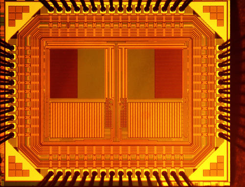
The research team has developed prototype CMOS active pixels that can simultaneously perform imaging and energy harvesting without the need to introduce additional planar PN junctions whose pixels use structures available in standard CMOS processes. The main author of the paper, Eusik Yoon, explained in the abstract of the paper: “Unlike conventional CMOS-based imaging pixels, the N-well region in the new sensor is used as a sensing node for image capture. We have adopted hole-based imaging technology. At the same time, the N-well region is used to collect energy with a high fill factor higher than 94%.
"Highest power density"
Euisik Yoon said: “We have successfully demonstrated that energy harvesting can achieve a power density of 998 pW/klux while capturing images at 74.67 pJ/pixel. Our current prototype device already achieves the highest power density and can achieve 15 The speed of the fps maintains its image capture without the need for an external power supply exceeding 60 klux of lighting."
According to the content of the paper, the new sensor will achieve a speed of 15 images per second under "clear weather of 60,000 lux" and 7.5 sheets per second under normal daylight conditions (usually 20,000 to 30,000 lux). The speed of image acquisition. According to reports, researchers are currently focusing on the development of proof-of-concept chips, and they pointed out in the paper that they have not optimized the power consumption of the sensors themselves.
The paper concludes: "We have proposed a prototype CMOS active pixel architecture that can simultaneously perform imaging and energy acquisition using a built-in embedded vertical PN junction in a standard CMOS process and use holes as imaging. The charge carriers achieve a high fill factor of 94%.To prove the feasibility of this design, we fabricated a CIS chip and conducted an energy harvesting test with a power density of 998 pW/klux, and at the same time generated a quality factor of 74.67 pJ/. The pixel image, which provides the highest power density.â€
(Original Title: Engineers at the University of Michigan Develop Solar Imaging Sensors)
Selective Laser Sintering
Selective Laser Sintering (SLS) was developed at the University of Texas in Austin, by Carl Deckard and colleagues. The technology was patented in 1989 and was originally sold by DTM Corporation. DTM was acquired by 3D Systems in 2001. The basic concept of SLS is similar to that of SLA. It uses a moving laser beam to trace and selectively sinter powdered polymer and/or metal composite materials into successive cross-sections of a three-dimensional part. As in all rapid prototyping processes, the parts are built upon a platform that adjusts in height equal to the thickness of the layer being built. Additional powder is deposited on top of each solidified layer and sintered. This powder is rolled onto the platform from a bin before building the layer. The powder is maintained at an elevated temperature so that it fuses easily upon exposure to the laser. Unlike SLA, special support structures are not required because the excess powder in each layer acts as a support to the part being built. With the metal composite material, the SLS process solidifies a polymer binder material around steel powder (100 micron diameter) one slice at a time, forming the part. The part is then placed in a furnace, at temperatures in excess of 900 °C, where the polymer binder is burned off and the part is infiltrated with bronze to improve its density. The burn-off and infiltration procedures typically take about one day, after which secondary machining and finishing is performed. Recent improvements in accuracy and resolution, and reduction in stair-stepping, have minimized the need for secondary machining and finishing.
The main material for the SLS are the metal part or Nylon material which are commonly used in the industry or consumer fields. contact us to do the business, we are your best partner from beginning to end to give you the best service.

Selective Laser Sintering,Laser Sintering,Selective Laser Sintering 3D Printing,Laser Sintering Service
Suzhou FCE precision electronics Co., LTD , https://www.fukeyifcesz.com